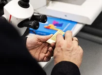
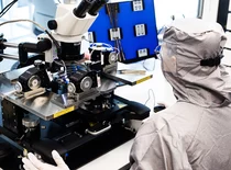
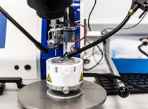
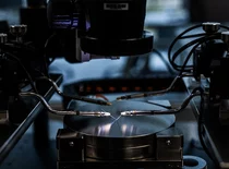
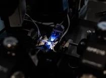
ProtoLAB is designed for rapid design, prototyping and testing of low-volume micro- and nano-electronic products. The lab is equipped with an ISO 5 cleanroom, Form Factor chip probing stations, Finetech Sigma chip building/welding, TPT wire welding and plasma surface etching equipment. Prototype enclosures and precision structural elements are realised with specialised 3D printing equipment. 3D printing uses materials that are rather complicated to process using traditional technologies: carbon fibre, ceramics, composite materials, etc. This type of equipment enables the production of non-standard, smart, biocompatible products in small quantities thanks to the prototyping and industrial design expertise concentrated at ProtoLAB. ProtoLab is a member of the Europractice network. The chips are designed and tested with the latest Cadence and Siemens EDA software.
Prototypes of chips and other micro/nano systems are realised using the production capacities of amsOSRAM, Fraunhofer IISB, GlobalFoundries, IHP, STMicroelectronics, TSMC, UMC, UMS, X-FAB, AMF, CORNERSTONE, IMEC, LioniX, Pragmatic, MEMSCAP. The prototyping service for researchers is provided by professional engineers with expertise in the relevant equipment. Prototype production takes between 3 and 12 months according to state-of-the-art standards and depending on the complexity of the prototype. The final prototypes can be put into production, optimised and tested for series production at Protolab Continental’s SMT centre.


